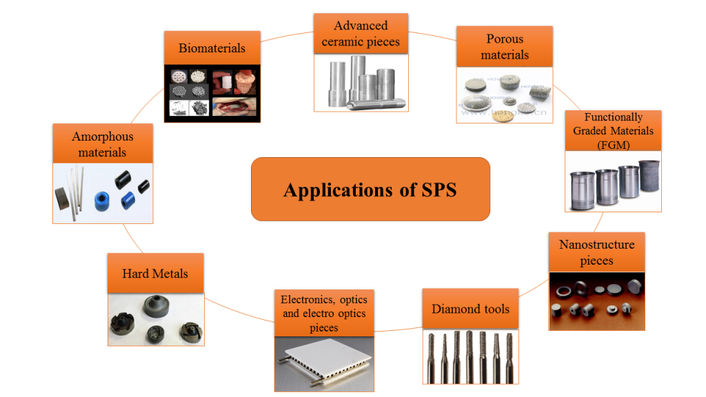

SPS technology is known as the most effective sintering method for nanostructured materials with the lowest grain growth rate and the least negative impact on the structure of the material. This method uses the simultaneous pulsed (on-off) direct electrical current (DC) and a uniaxial compressive force for the sinter. The simultaneous use of pressure and heat will reduce the temperature and time of the sinter and thus improve the mechanical, electrical and magnetic properties of the bulk pieces obtained through this method. This method has the ability to sinter all types of conductive and non-conductive materials
Mechanism of the SPS process
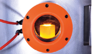
When a spark discharge appears through the empty space between particles, a local high temperature-state is generated momentarily (Joule heat). As the temperature rises, the impurities evaporate and areas of the particles surface melt. The particles are bonded to each other under the influence of applied pressure, and as the process continues, the sintering process is completed
Sintered Samples
SiC- B4C- HfB2– TiB2– ZrB2– SiAlON-TaC-WC-Si3N4
Ta- Ti- Cu- Al-Mg
HEA-Co/Fe2O3-Cu/CNT-Ti/NaCl-Ti/Hydroxyapatite-Al/SiC-Al/WS2