
Thin Film Deposition is the technology of applying a very thin film of material – between a few nanometers to about 100 micrometers,or the thickness of a few atoms – onto a “substrate” surface to be coated, or onto a previously deposited coating to form layers. Thin Film Deposition manufacturing processes are at the heart of today’s semiconductor industry, solar panels, CDs, disk drives, and optical devices industries
Thin Film Deposition is usually divided into two broad categories :
1-Chemical Vapor Deposition (CVD) Coating Systems
2-Physical Vapor Deposition (PVD) Coating Systems
Chemical Deposition is when a volatile fluid precursor produces a chemical change on a surface leaving a chemically deposited coating. One example is Chemical Vapor Deposition or CVD used to produce the highest-purity, highest-performance solid materials in the semiconductor industry today
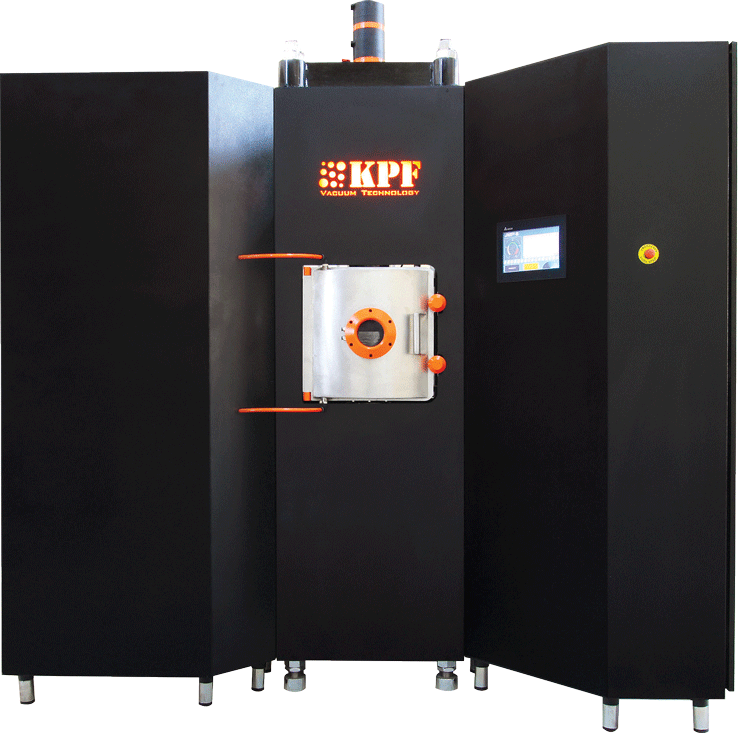
Physical Vapor Deposition (PVD) refers to a wide range of technologies where a material is released from a source and deposited on a substrate using mechanical, electromechanical or thermodynamic processes
source